-
Manufacturing Process of LED Chip
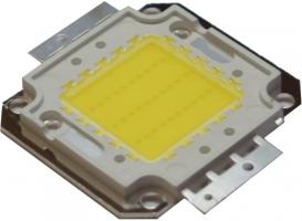
The basic manufacturing Process of LED Chip is shown below.
Epitaxial wafer → cleaning → plating transparent electrode layer → transparent electrode pattern lithography → corrosion → debonding → platform pattern lithography → dry etching → degraction → annealing → SiO2 deposition → window pattern lithography →SiO2 corrosion → degglomerate → N-pole pattern lithography → pre-cleaning → coating → stripping → annealing → P-pole pattern lithography → coating → stripping → grinding → cutting → chip → finished product testing.

In fact, the production process of the epitaxial wafer is very complicated. After the epitaxial wafer is finished, the next step is to make the electrode (P pole, N pole) of the LED epitaxial wafer, and then start cutting the LED epitaxial wafer with a laser machine (previously cutting LED epitaxial wafers are mainly made of diamond knives. After being fabricated into chips, nine points are taken at different positions on the wafer for parameter testing:
1. Test the voltage, wavelength and brightness mainly. The wafer that meets the normal shipping standard parameters will continue to do the next step. If the nine-point test does not meet the relevant requirements, the wafer will be set aside.
2. After the wafer is cut into chips, 100% of the visual inspection (VI/VC) is performed by the operator using a microscope magnified 30 times.
3. Then use the fully automatic sorting machine to fully select, test and classify the chips according to different voltage, wavelength and brightness prediction parameters.
4. Finally, check (VC) and label the LED chip. The chip area should be at the center of the blue film. There should be up to 5,000 and no less than 1000 chips on the blue film. Chip type, lot number, quantity, and photometric statistics are recorded on the label and attached to the back of the glossy paper. The chip on the blue film will be the same as the first visual inspection standard, ensuring that the chips are neatly arranged and of good quality. This makes LED chips (currently known as square chips on the market).
In this way, LED chips are produced (currently collectively referred to as square chips on the market).
Stanford Advanced Materials (SAM) Corporation is a global supplier of various sputtering targets such as metals, alloys, oxides, ceramic materials. We provide high purity of semiconductor materials, which are important raw materials for LED chip manufacturing. If you are interested, please visit our website https://www.sputtertargets.net/ for more information.
 Tags : led chip, semiconductors, cpu
-
Commentaires
