-
Plasma spraying is a physical vapor deposition method, other pvd methods includes magnetron sputtering and vacuum evaporation.
The plasma spray equipment power supply uses three opposite star thyristor (SCR) rectifier power supplies. The power supply is small in size, light in weight, easy to move and stable in performance, safe and reliable in operation, especially suitable for large-scale on-site construction work.
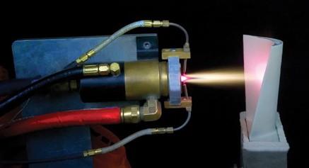
The starting arc current and working current of the equipment can be arbitrarily set and adjusted at any time. The arcing current can automatically transition to the working current, and the power supply is air-cooled.
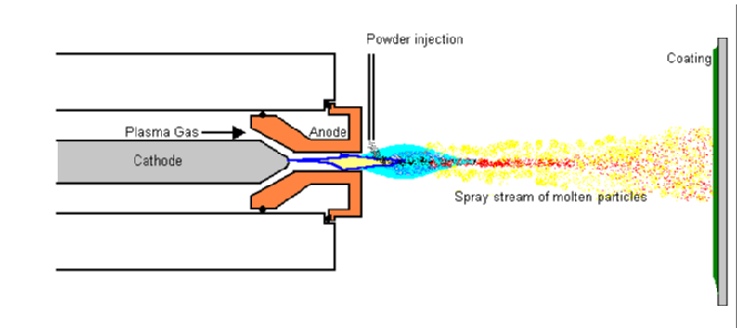
The plasma spray gun has two types: a hand-held gun (included in the device) and a machine gun (optional), and the spray guns are all internal powder feeding type. The powder injection point temperature is as high as 7000-8000 °C, which is 2000-4000 °C higher than the powder injection point temperature of the conventional powder delivery gun under the same conditions, which improves the energy utilization rate of the whole machine.
The working gas is mainly N2 (nitrogen) plus ordinary H2 (oxygen), and Ar (argon) or Ar (argon) plus H2 (hydrogen) can also be used as the working gas. Since a diatomic gas is used as the working gas, the plasma jet flame value is high.
Because the equipment uses an internal powder gun and a common purity diatomic gas as the working gas, the operating cost is greatly reduced.
Reasonable design of the spray gun structure and configuration of the preferred process parameters greatly extend the life of the gun consumables (nozzles and cathodes). Even in the case of a cooling water temperature of 40 ° C, the cumulative life of the nozzle can reach 50-100 hours. At the same time, the wearing parts are easy to replace, and the cathode can be repaired and used many times.
The whole machine can work continuously for more than 8 hours. And the spraying speed is high, taking the example of spraying Al2O3, the coating thickness is 0.1mm, and the area of 2 square meters can be sprayed per hour.
The powder feeder has a gravity type (transporting a naturally flowing powder) and a scraper type (delivering a powder with a poor natural fluidity), and the user can select one of them according to the needs of the spray.
Please visit https://www.sputtertargets.net for more information.
 votre commentaire
-
Definition
Sputtering is a kind of preparation technology of PVD (physical vapor deposition) thin film. Sputtering can be mainly divided into four categories: DC sputtering, AC sputtering, reactive sputtering and magnetron sputtering.
Principle
Sputtering uses a high-speed movement of positive ions generated by gas discharge under the action of an electric field to bombard the cathode target, causing atoms or molecules in the solid sputtering target to escape and deposit on the surface of the workpiece to be formed, thereby forming a film.
Use
Electronics industry develops fast and requires high purity and large quality materials. The production of computer hard disks is an important and widespread application of sputtering deposition. Sputtering can also deposit the metal (such as aluminium) layer during the fabrication of CDs and DVDs
Sputtering target is also used extensively in the semiconductor industry to deposit thin films of various materials in integrated circuit processing. And those sputtering targets used in semiconductor industries are specially called Anelva targets. Anelva targets can make the surface of metal, alloy or dielectric film on the surface of the base material. Suitable for manufacturing thin film integrated circuit, chip lead device and semiconductor device.

Optical coating, for instance, thin antireflection coatings on glass for optical applications, is also an important application of sputtering can also be used to sputter. Because of the low substrate temperatures used, sputtering is an ideal method to deposit contact metals for thin-film transistors. Another familiar application of sputtering is low-emissivity coatings on glass, used in double-pane window assemblies, which is a multilayer containing silver and metal oxides such as zinc oxide, tin oxide, or titanium dioxide.
A large industry has developed around tool coating using sputtered nitrides, such as titanium nitride, which has the similar color with gold, to create the gold colored hard coat. It is really an economical choice.
Method
Sputtered thin films are usually produced in the plasma of inert gas (such as argon).
Features
The sputtering process has the advantages of low substrate temperature, thin film quality, uniform and compact structure, good firmness and reproducibility. Another important advantage of sputter deposition is that even materials with very high melting points can be easily sputtered.
Please visit https://www.sputtertargets.net/ for more information.
votre commentaire
-
Target bonding is a very important step in sputter coating, which extends the life of the target and improves the performance of the target. Target bonding, as its name suggests, is the welding of the sputtering target to the back target. Generally speaking, there are three main ways to achieve target bonding: crimping, brazing and conductive adhesives.

Methods
Crimp: In order to improve the contact quality, graphite paper, Pb or In leather are used.
Brazing: Generally, in the case of using a solder material, a sputtering power of less than 20 W/cm 2 is required, and In is commonly used.
Conductive adhesive: The conductive adhesive used should be resistant to high temperatures and have a thickness of 0.02-0.05 μm.
Application
Technically, targets with a flat surface and can be metallized can be bonded to improve the heat dissipation and target utilization of the sputtering process. It is suitable for brittle targets such as ITO, SiO2, ceramics, and sintered targets; soft metal targets such as tin and indium; and the case where the target is too thin and the target is too expensive.
Requirements of the Back Targets
The back target is generally selected from oxygen-free copper and molybdenum targets with a thickness of about 3 mm. It requires good electrical conductivity, sufficient strength, hollow or solid structure, and moderate thickness (2-3 mm or so, too thick, and consumes part of the magnetic strength; too thin, easily transformed).

Back target shedding
The back target shedding may be caused by the following reasons: the sputtering temperature is too high, so that the oxygen-free copper is oxidized and warped; the current is too large and the heat conduction is too fast, so that the temperature is high, under which condition the welding material is easily melted; the circulating water temperature is high, and the heat dissipation is not good; the density of the target itself is too high, so that the back target is not easily adsorbed.
Stanford Advanced Materials is devoted to machining standard backing plates and working together with the Taiwan Bonding Company for providing bonding services. For more information please visit https://www.sputtertargets.net/. For more questions about target bonding materials, methods and services, please see our listing of frequently asked questions (FAQs).
votre commentaire
-
Molecular beam epitaxy is a new crystal growth technique, abbreviated as MBE. In an ultra-high vacuum chamber, the source material is subjected to high-temperature evaporation, glow discharge ionization, gas cracking and electron beam heating evaporation to generate a molecular beam current. After the incident molecular beam exchanges energy with the substrate, it is adsorbed, migrated, nucleated and grown to form a film.
Molecular beam epitaxy mainly studies the growth of crystals and superlattices of different structures or different materials. The growth system is equipped with a variety of monitoring equipment to perform instantaneous measurement and analysis of substrate temperature, growth rate, and film thickness during growth. At the same time, the growth details such as surface irregularities, undulations, atomic coverage, adhesion coefficient, evaporation coefficient and surface diffusion distance are accurately monitored.

Molecular beam epitaxy was developed from the preparation of semiconductor thin film materials by vacuum evaporation technology in the 1950s, and has been improved by the development of ultra-high vacuum technology. The development of molecular beam epitaxy has opened up a series of new superlattice devices and expanded a new field of semiconductor science, which further illustrates the impact of the development of semiconductor materials on semiconductor physics and semiconductor devices.
The advantage of molecular beam epitaxy is that it can prepare ultra-thin layer of semiconductor materials; the surface of the epitaxial material has good surface morphology and large uniformity; it can be made into multilayer structures with different dopants or different compositions; The temperature of epitaxial growth is low, which is beneficial to improve the purity and integrity of the epitaxial layer; the growth environment is clean and the pollution is small.
Stanford Advanced Materials (SAM) Corporation is a global supplier of various sputtering targets such as metals, alloys, oxides and ceramic materials, which are widely used in multiple industries. We regularly update knowledge and interesting stories of sputtering targets on our website. If you are interested, please visit https://www.sputtertargets.net/ for more information.
votre commentaire
-
The basic manufacturing Process of LED Chip is shown below.
Epitaxial wafer → cleaning → plating transparent electrode layer → transparent electrode pattern lithography → corrosion → debonding → platform pattern lithography → dry etching → degraction → annealing → SiO2 deposition → window pattern lithography →SiO2 corrosion → degglomerate → N-pole pattern lithography → pre-cleaning → coating → stripping → annealing → P-pole pattern lithography → coating → stripping → grinding → cutting → chip → finished product testing.
In fact, the production process of the epitaxial wafer is very complicated. After the epitaxial wafer is finished, the next step is to make the electrode (P pole, N pole) of the LED epitaxial wafer, and then start cutting the LED epitaxial wafer with a laser machine (previously cutting LED epitaxial wafers are mainly made of diamond knives. After being fabricated into chips, nine points are taken at different positions on the wafer for parameter testing:
1. Test the voltage, wavelength and brightness mainly. The wafer that meets the normal shipping standard parameters will continue to do the next step. If the nine-point test does not meet the relevant requirements, the wafer will be set aside.
2. After the wafer is cut into chips, 100% of the visual inspection (VI/VC) is performed by the operator using a microscope magnified 30 times.
3. Then use the fully automatic sorting machine to fully select, test and classify the chips according to different voltage, wavelength and brightness prediction parameters.
4. Finally, check (VC) and label the LED chip. The chip area should be at the center of the blue film. There should be up to 5,000 and no less than 1000 chips on the blue film. Chip type, lot number, quantity, and photometric statistics are recorded on the label and attached to the back of the glossy paper. The chip on the blue film will be the same as the first visual inspection standard, ensuring that the chips are neatly arranged and of good quality. This makes LED chips (currently known as square chips on the market).
In this way, LED chips are produced (currently collectively referred to as square chips on the market).
Stanford Advanced Materials (SAM) Corporation is a global supplier of various sputtering targets such as metals, alloys, oxides, ceramic materials. We provide high purity of semiconductor materials, which are important raw materials for LED chip manufacturing. If you are interested, please visit our website https://www.sputtertargets.net/ for more information.
votre commentaire Suivre le flux RSS des articles Suivre le flux RSS des commentaires


|
|
|
|